CLOSE
About Elements
田中贵金属是贵金属领域的翘楚企业。
支撑社会发展的先进素材和解决方案、
创造了这些的开发故事、技术人员们的心声、以及经营理念和愿景——
Elements是以“探求贵金属的极致”为标语,
为促进实现更加美好的社会和富饶的地球未来传播洞察的网络媒体。


Enhancing the Reliability of Precious Metals for Brazing Filler Metals in Power Devices
Welding Technology, June 2022
Takaomi Kishimoto(TANAKA Kikinzoku Kogyo K.K.)
1. Introduction
A power device is a semiconductor used to convert electric power, and its diverse applications include cars, renewable energy, and industrial equipment. Demand for these devices has been growing each year, particularly in car applications, backed by increased adoption of hybrid and electric vehicle. With development efforts also advancing on the performance front for increased efficiency, miniaturization, and higher output, there have been calls for each power device component to enhance its performance and reliability to withstand harsher operating environments.
Figure 1 shows the structure of a power device. A power device consists of multiple components which are made from various materials such as semiconductors, metals, and ceramics. The components are joined, with different materials joining together at multiple interfaces. When power devices are not operating (for example, when a car is parked), they cool down to levels near outdoor temperatures. Particularly during the winter, their temperatures may drop to subzero conditions; even as low as several 10s of degrees Celsius below zero, depending on the region. In contrast, once a car starts running, electricity flows through the power device. This generates heat and the temperature may reach several 10s of degrees above 100 degrees Celsius. The operation of power devices thus creates a cycle of heat generation and cooling and repeatedly applies thermal shock to power device components and their joints, causing particularly strong forces on the joints of different materials.

Figure 1. Power device structure
Among the components of a power device is a ceramic circuit board. A ceramic sheet with copper (Cu) sheets joined on both sides, the front side of the circuit board features an electrical circuit function and the underside serves to dissipate heat. While providing electrical insulation between the electrical circuit and cooling device, the ceramic sheet in the middle performs an important role by conducting heat generated by the semiconductor chip to the cooling device. The heat generated by the operation of the power device causes the Cu joined on the ceramic sheet surface to significantly expand, and once the device stops operating, the Cu cools down and contracts. Ceramics, in contrast, exhibit very little expansion from heat. As such, in a ceramic circuit board, only the Cu sheets cycle through expansion and contraction, with stress from the cycle generated by thermal expansion and contraction continuously being applied to the joint interface with ceramics. Moreover, whereas the operating temperature of power devices has conventionally been set to a maximum of around 150℃, there is growing need in the future for operating under higher temperatures such as 175℃ or 200℃.1 Demand is thus growing daily for ceramic circuit boards that feature thermal shock resistance and reliability. Furthermore, the general approach so far has been to join approximately 0.3 mm thick Cu sheets with a ceramic sheet. However, there is increasing demand for better performance of ceramic circuit boards, including ongoing attempts to use 0.8 mm or thicker Cu sheets for better heat dissipation.
This present provides a report on the studies that have been made on enhancing the reliability of ceramic circuit boards, which are a component of power devices.
2. Background and objective of application
Brazing is one of the several methods available for joining a ceramic sheet to Cu, which are used in a ceramic circuit board.
In general, brazing is employed to join metals. This means ceramics cannot be joined through brazing, but a special brazing filler called an active brazing filler metal allows for direct brazing of ceramics. An active metal is a brazing filler that has improved wettability with ceramics through the introduction of additive elements such as titanium and other types of active metals. Active brazing filler metals consisting of silver (Ag) and Cu added with titanium (Ti) are widely known and used also in the manufacturing of ceramic circuit boards.
Figure 2 shows the manufacturing method of a ceramic circuit board. First, note that the joining process here uses active brazing filler metal in paste form. The brazing paste, made by kneading the metal powders of Ag, Cu, and Ti with an organic solvent, is applied on ceramic sheets, such as silicon nitride, onto which a Cu sheet is placed. They are then vacuum-heated to melt the paste and braze the sheets. Here, a eutectic AgCu alloy would allow for brazing at around 800℃ as its melting point is 780℃. However, the brazing paste employed in this process consists of a mixture of Ag, Cu, and Ti powders, as mentioned above, and does not melt when heated to 800℃. Brazing is thus performed by heating to 900℃ or above, which is near the melting point of Ag.
Once the brazing is complete, Cu is joined to both sides of the ceramics. The Cu on one side, however, is subsequently removed through an etching process as a circuit pattern needs to be formed there. To form the circuit pattern, the Cu has its surface masked and undergoes chemical etching, after which the brazing filler layer is etched as well. These processes result in a completed ceramic circuit board.

Figure 2. Ceramic circuit board manufacturing method (current)
The use of this method to manufacture ceramic circuit boards, however, generates some concerns as to reliability. One is the impact of the high brazing temperature (900℃ or above); the second is the damage that etching inflicts on ceramics.
Regarding the high brazing temperature, ceramics generally have a lower thermal expansion coefficient than metal. When cooled after high-temperature brazing, the difference between the thermal expansion coefficient of ceramics and metal would cause significant residual stress on the joint interface. Subsequently, the joint interface will experience repetitive thermal shock with each instance of power device operation, as mentioned in the introduction of this article. Considering that the interface is already exposed to significant stress in its post-brazing state, it is desirable to lower the brazing temperature to the extent possible and suppress Cu expansion, and thereby reduce stress generation in the joint interface with ceramics. This, however, is difficult as the process uses brazing paste that was obtained through kneading Ag, Cu, and Ti powders.
Next, regarding the damage from etching, the interface between ceramics and Cu is joined by a brazing filler layer, and on the interface between the ceramics and the brazing filler layer is a Ti compound layer that is formed through a compositional reaction of ceramics and Ti in the active brazing filler metal. Residual brazing filler and Ti compound layers on the surface of ceramics could cause failure in establishing insulation between circuit patterns and allow electricity to flow to unexpected locations, which means these layers need to be fully removed. Currently the Ti compound removal process uses ammonium fluoride, among other sources. Whereas this method can remove Ti compounds, it may damage the ceramic substrate and silicon nitride and consequently impair reliability.
Conventional processes thus entail some concerns that are expected to develop into issues down the road when demands arise for greater resistance and reliability. As such, there is a need to develop a new ceramic circuit board manufacturing method that can solve these problems.
3. Details of technology
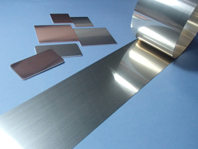
To solve the aforementioned issues, studies were conducted on a ceramic circuit board manufacturing method that can lower the brazing temperature without the need for an etching process. A solution that was examined and described herein concerns the use of active brazing filler metals/Cu clad materials (i.e., a cladding of active brazing filler metals with Cu materials). Figure 3 shows a photo of active brazing filler metals/Cu clad materials, which have a thin active brazing filler metal layer laminated on one side of the Cu sheets. The metals/materials were manufactured through punch pressing, following a successive lamination process of Cu and active brazing filler metal sheets. The Cu and brazing filler metal are 0.8 mm and 20 µm thick, respectively.

Figure 3. Active brazing filler metal/copper clad material press pieces
This composite used an AgCuSnTi alloy as its brazing filler metal. As mentioned earlier, brazing filler metals consisting of Ag, Cu, and Ti are commonly known, and AgCuSnTi alloy-based brazing filler metal sheets are also available on the market. Attempts to obtain foil by processing dissolved and cast AgCuSnTi alloy into sheet form, however, generate large particles of CuTi compound in the metal structure, as shown in Figure 4. Given the extremely hard nature of the large particles, further processing will make the particles penetrate through to or fall out from the sheet surface, causing fractures/holes. This has created difficulties in processing the AgCuSnTi alloy into thin sheet and foil forms, and, naturally, it was also not possible to laminate the alloy with Cu.

Figure 4. Metal structure cross section of active brazing filler metals
As such, studies have previously been made on the potential for achieving improved metal structure by introducing additives to the AgCuSnTi alloy. Results showed that doing so with AgCuSnTi alloy enables fine Ti compound dispersion, and this led to the development of AgCuSnTi alloy-based active brazing filler metals. Using this AgCuSnTi alloy allowed for prototyping the aforementioned clad materials in this article.
Figure 5 shows the manufacturing process of a ceramic circuit board that uses active brazing filler metals/Cu clad materials. The first step is to prepare active brazing filler metals/Cu clad materials that have been pressed into desired forms (e.g., circuit, heat sink), and place them on a ceramic sheet. The metals/materials can be positioned by using carbon jigs and other such tools. Then the composite is heated in a vacuum furnace to braze the ceramic sheet to the metals/materials. Considering that the brazing filler metals used herein have an approximately 750℃ melting point and are alloys, they do not require heating to 900℃ or above unlike the aforementioned brazing paste. This has allowed for lowering the brazing temperature to 800℃. In addition, no post-brazing etching process is necessary because the active brazing filler metals/Cu cladding materials have been pressed into desired forms in advance, thereby eliminating both the need for an etching process and concerns about the damage that an etching process may inflict on ceramics. As such, concerns over the aforementioned conventional processes are thought to have been resolved through the use of the new manufacturing process that harnesses active brazing filler metals/Cu clad materials.

Figure 5. Ceramic circuit board manufacturing method (prototype)
4. Achievements to date
Figure 6 shows a sample of a ceramic circuit board on which brazing has actually been performed using active brazing filler metals/Cu clad materials.

Figure 6. Ceramic circuit board manufactured using active brazing filler metals/copper clad materials
This sample used a composite material with a dimension of 0.8 × 30 × 30 mm (20 µm brazing filler metal layer) and the thickness of silicon nitride is 0.32 mm.
Figure 7 shows observation results on the state of the interface, following its joining process. The observations were made with a transmission electron microscope (TEM). The TEM observation results showed that Ti gathered near the ceramics and that the Ti layer formed uniformly across the entire joint interface. This Ti layer, furthermore, consisted of TiN and Ti5Si3 in the order of proximity from the silicon nitride. These compounds generally occur when silicon nitride joins with active brazing filler metals.2 Brazing is thus considered to have been achieved through a reaction of the active brazing filler metal of the AgCuSnTi alloy and silicon nitride. Also, a previous study reported that when nitride ceramics are joined with active brazing filler metals, excessive TiSi layer formation on the joint interface may cause the strength of the joint to decrease,3 but the joint achieved herein only saw partial and discontinuous Ti5Si3 layer formation despite a TiNi layer having formed across the entire joint interface. It is considered that the Ti5Si3 layer has no risk of becoming brittle and negatively impacting the reliability of the joint, and that the joint is in a good state.

Figure 7. TEM observation results of silicon nitride/active brazing filler metal joint interface
A heat cycle test was subsequently performed to evaluate reliability. An evaluation test simulating power device operation, this test cyclically moves a test sample between cooling and heating chambers to apply thermal shock and evaluate its thermal shock resistance. The test conditions set herein were a -50℃ cooling chamber and 175℃ heating chamber, a 30-minute retention time per chamber, and one hour per cycle. The evaluation employed an ultrasonic flaw inspection method to measure the state of the test sample, both after brazing and every 250 cycles of the heat cycle test.
Figure 8 shows results of the heat cycle test.

Figure 8. Heat cycle test results (ultrasonic flaw inspection)
No void or material detach were identified shortly after brazing or before the heat cycle test, and the entire surface of the Cu and ceramic sheets were confirmed to have joined together. The state of the joint also remained unchanged after 250 and 500 cycles; no change was identified even after 1,500 cycles. This confirmed that the ceramic circuit board features sufficient thermal shock resistance, and as such, ceramic circuit boards manufactured with active brazing filler metals/Cu composites are considered to have high thermal shock reliability.
5. Future applications
Further lowering the brazing temperature is considered one solution to ensure even higher levels of reliability, and efforts are currently underway to optimize the composition of brazing filler metals to reduce the brazing temperature. Improving heat dissipation performance is also considered necessary, given that power devices are expected to further miniaturize and increase in power density. A double-sided cooling structure is being studied as a solution. Figure 9 shows an example application of such a structure. Heat from semiconductor chips has conventionally been released only downward, but situating ceramic circuit boards on both sides will allow heat to be released both upward and downward and thereby enhance heat dissipation performance. In relation to this, a process to form terminals and circuit patterns concurrently on the ceramic circuit board surface is also being studied. Given that active brazing filler metals/Cu clad materials can be pressed into any form, manufacturing such terminal-featuring forms would be easy and allow for capitalizing on the features of the metals/ materials.

Figure 9. Example application of active brazing filler metals/copper clad materials
6. Summary
There are concerns that conventional manufacturing methods are rendering ceramic circuit boards, which are a component of power devices, increasingly unreliable due to high-temperature brazing and chemical damage that occurs on ceramics during etching processes. Ceramic circuit boards may thus become incapable of coping with harsher operating environments that are expected in the future.
To solve these issues, active brazing filler metals/Cu clad material brazing fillers have been developed and studies were conducted on lowering the brazing temperature and a process that eliminates the need for etching.
The brazing temperature was successfully reduced to 800℃, down 100℃ from the conventional 900℃-or-above level. An etching-free process has been attained as well by pressing and forming active brazing filler metals/Cu cladding materials into a circuit before the brazing process. A ceramic circuit board sample, manufactured with this new process, was subjected to a heat cycle test evaluation and the results showed that the sample can resist 1,500 cycles or more in -50℃ to 175℃ test conditions. The manufacturing of a highly reliable ceramic circuit board that can withstand harsh operating conditions expected in the future is thus considered to have been achieved.
Also, plans are underway to keep advancing various developmental efforts, such as clad material applications and active brazing filler metal optimizations. These efforts include the further reduction of brazing filler temperatures and a double-sided cooling structure for better heat dissipation performance. It is hoped that these technologies will lead to enhanced power device reliability and more efficient use of energy, and thereby contribute to the future of our beautiful planet.
References
1)Supervisor Katsuaki SUGANUMA:System Integration of Wide Band Gap Semiconductors
2)Yushi SHICHI:Journal of the Ceramic Society of Japan 97 [11] 1354-57 (1989)
3)Kimiaki NAGATSUKA:Quarterly Journal of the Japan Welding Society Vol. 31 No. 1 p.16-22 (2013)