CLOSE
About Elements
田中贵金属是贵金属领域的翘楚企业。
支撑社会发展的先进素材和解决方案、
创造了这些的开发故事、技术人员们的心声、以及经营理念和愿景——
Elements是以“探求贵金属的极致”为标语,
为促进实现更加美好的社会和富饶的地球未来传播洞察的网络媒体。


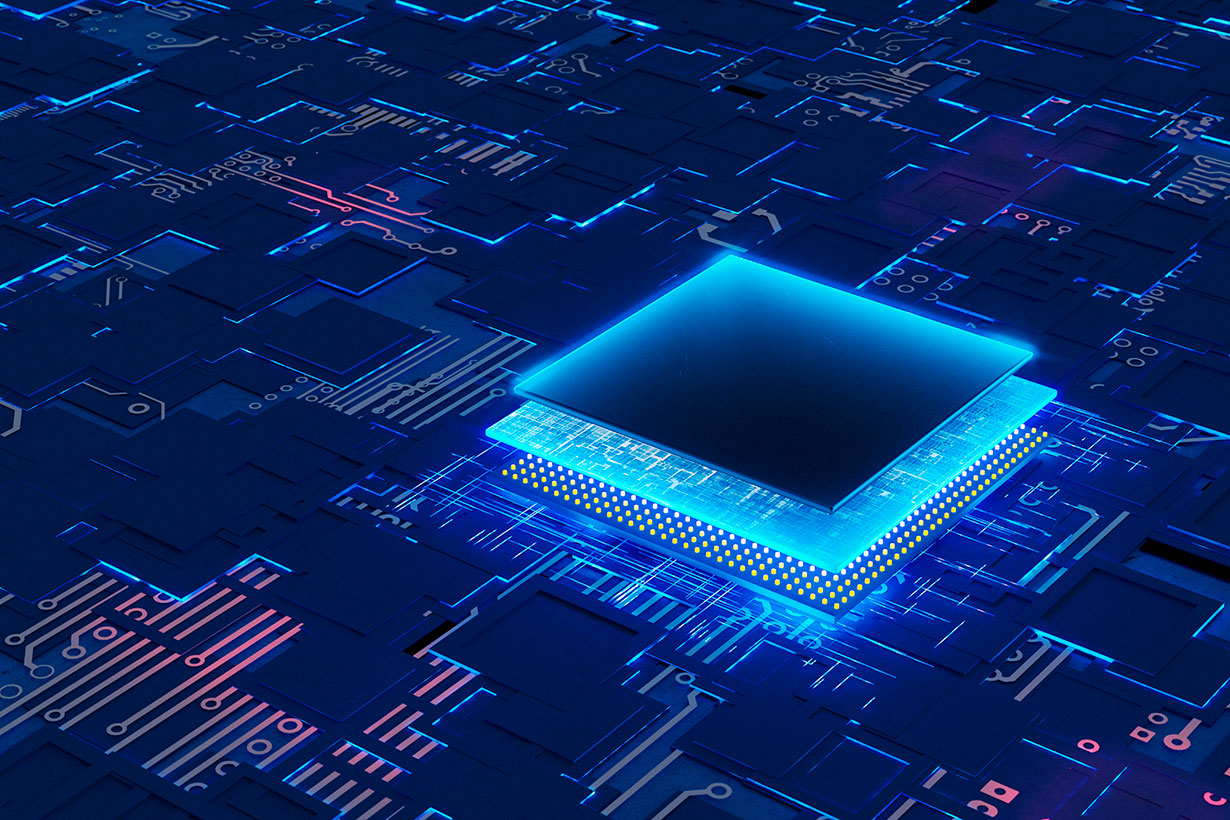
A step forward in the quest to replace silicon with 2D chips
Two-dimensional semiconductors have a chance to galvanize significant advances in electronic device capabilities, replacing silicon-based chips. However, many problems continue to hold back these devices.
A major problem is carrier mobility, or how fast electrons can move through the semiconductors. These 2D semiconductors are notoriously slow in this area, limiting the ability for improvements and real-world applications.
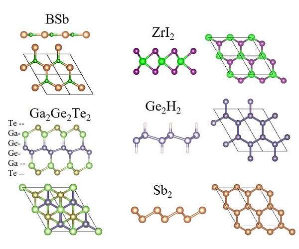
Researchers at The University of Texas at Austin have discovered more than a dozen different materials for 2D semiconductors that could allow electrons to quickly move around, which opens the door for a leap in electronics’ capabilities.
Representative 2D semiconductors with very high charge mobility at room temperature
“If you can replace silicon with 2D semiconductors that will lead to faster devices that consume significantly less energy,” said Yuanyue Liu, an assistant professor in the Cockrell School of Engineering’s Walker Department of Mechanical Engineering and Texas materials Institute, who leads the project.
The research was recently published in Physical Review Letters.
The big difference between traditional silicon-based semiconductors and 2D semiconductors is their geometry. The 2D semiconductors are much thinner, only a couple of atomic layers thick. This is advantageous in many ways as the push to make semiconductors smaller continues to pick up steam.
The compact nature of 2D semiconductors creates problems as well. The electrons are packed in tight, without much freedom to move. Scattering sources can more easily knock them off track in these smaller spaces, which is why carrier mobility is generally low in 2D semiconductors, preventing improved power and efficiency.
The 14 materials discovered by the researchers with high carrier mobility are an exception to this problem. Unique properties among these materials make the electrons more transparent, rendering them essentially invisible to scatterings and allowing the electrons to stay on course.
To find these materials, the researchers used an existing materials database and a checklist of characteristics that they hypothesized would lead to improved mobility. They then used quantum-mechanical method to accurately calculate the carrier mobility in the materials.
“The fact that we only found 14 materials with potentially high carrier mobility out of thousands does not contradict the conventional wisdom,” Liu said. “It shows how difficult it is to find 2D semiconductors with high carrier mobility.”
The next step, Liu says, is to partner with experimental researchers and work on fabricating materials to test and verify their findings. Though Liu is confident in the findings, he cautioned that they are still theoretical and will need to be confirmed by real-world testing.
Other team members on the project include Chenmu Zhang, Ruoyu Wang and Himani Mishra, all from the Walker Department of Mechanical Engineering and the Texas Materials Institute.
Research Report:Two-Dimensional Semiconductors with High Intrinsic Carrier Mobility at Room Temperature
This article was from SpaceDaily.com and was legally licensed through the Industry Dive Content Marketplace. Please direct all licensing questions to legal@industrydive.com.
![]()